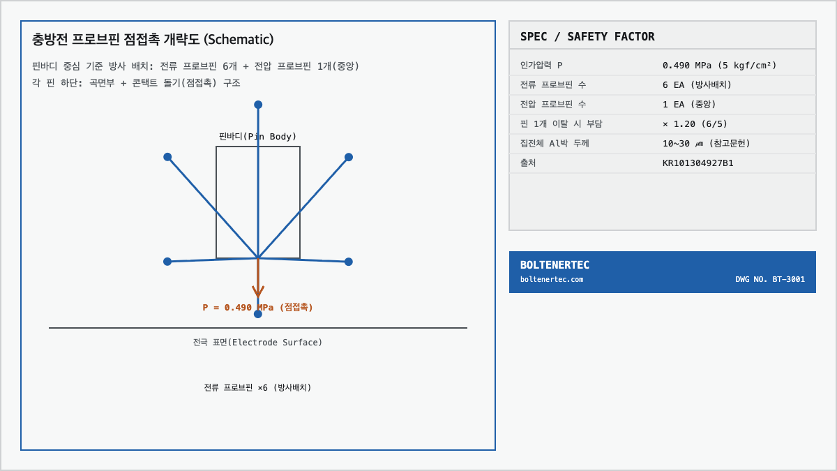
The contact pressure and pin-arrangement structure of the charge/discharge probe pin used in the formation process were reviewed based on the KR101304927B1 specification. It is a combined structure of 6 current probe pins and 1 voltage probe pin, with the applied pressure specified as “approximately 5 kgf/cm².”
Problem Definition
In the formation process of pouch-type lithium-ion cells, the charge/discharge probe pin contacts the electrode tab directly to apply current and voltage. If pin arrangement and applied pressure are inadequate, contact-resistance variation causes uneven cell charging, electrode tab damage, and pin wear. KR101304927B1 addresses this with a structure arranging 6 current probe pins circumferentially on the pin body, with 1 voltage probe pin placed in the central pin mount (KR101304927B1, specification).
Kinematic Analysis
The pin body consists of 6 pin mounts for current probe pins and 1 central pin mount for the voltage probe pin. The 6 pins are arranged evenly in the circumferential direction, forming point contacts across the front face of the electrode tab, and the central voltage pin, electrically separated from the current path, reduces voltage-drop measurement error in a manner similar to a 4-terminal (Kelvin) measurement method (KR101304927B1, specification).
Formula Verification
Converting the applied pressure stated in the specification, “approximately 5 kgf/cm²,” to SI units (MPa) gives the following.
$$P = 5 \, \text{kgf/cm}^2 \times 0.0980665 \, \text{MPa/(kgf/cm}^2\text{)} = 0.490 \, \text{MPa}$$
$P$: applied pressure per probe pin (MPa = N/mm²)
Letting the contact cross-sectional area of one pin be $A$ (mm²), the contact load $F$ per pin is calculated with the following equation.
$$F = P \times A$$
$F$: contact load (N), $P$: pressure (MPa), $A$: contact cross-sectional area (mm²) — however, the pin tip shape and cross-sectional area $A$ are not numerically stated in the specification and require confirmation.
When the 6 current pins make simultaneous contact, load can concentrate unevenly on some pins due to assembly tolerance and pin-body flatness deviation, so a load-redistribution coefficient $k$ is applied based on the single pin bearing the maximum load, to secure design margin.
$$F_{max} = k \times F_{avg}, \quad k = 1.20 \text{(estimated — a practical margin assumption for assembly tolerance and flatness deviation, not based on literature)}$$
Dual Safety-Factor Verification
- 1st — pin/tab contact-surface yield safety factor: per KR20140136950A, the pouch-cell electrode tab (current-collector aluminum foil) thickness range is stated as “more preferably 10 to 30 µm,” with the example embodiment at 20 µm. However, since this is a separate document from this formation-process patent (KR101304927B1), applying this thickness value is an assumption following comparable current-collector specifications (estimated), and the aluminum yield strength figure is unstated in both documents and requires confirmation.
- 2nd — pin wear safety factor: probe pin material and hardness data are not stated in the specification and require confirmation.
- Conclusion — because the material property values needed to calculate yield and wear safety factors are absent from the patent literature, quantitative safety-factor figures are withheld, and this verification is limited in scope to the pressure and load calculations.
Shop-notes
- When machining the pin-arrangement jig, the positional tolerance of the 6 pin mounts must be managed within ±0.05 mm to minimize load variation among the circumferentially arranged pins. (Machinability: wire EDM or a combination of precision drilling plus reaming is recommended; using a 6-hole simultaneous-machining jig makes it easier to secure positional tolerance.)
- The voltage probe pin must be electrically insulated from the current path to maintain 4-terminal measurement accuracy.
- Aluminum yield strength and pin-wear safety factor require separate verification once in-house measured data is secured.
One-line summary: The formation-process probe pin makes 6+1 contact at approximately 0.490 MPa (5 kgf/cm²) per KR101304927B1, but the material property values needed to calculate yield and wear safety factors are unstated in the literature and remain an item requiring confirmation.